


AuxeinAuxeinby Bucket Labs
AI Simulation for Semiconductor Manufacturing

Accelerating SemiconductorMaterial Yields withAI Simulation

Bucket Labs merges artificial intelligence with computational physics to optimize complex manufacturing methods like Bridgman, Czochralski, and Kyropoulos. Maximize your yields, reduce structural defects, and improve your semiconductor materials using AI-driven optimization and digital twin technology.

Request a Yield Optimization Audit
NVIDIAMember of NVIDIA Inception
Years to WeeksOptimization Timeline
IncreaseProcess Capabilities
Reduce WasteThrough Increase in Yield
ContinuousAI Model Improvement

Every chip begins as a single crystal

Every chip begins as a single crystal. Before a transistor is patterned, before a wafer is cut, there is one continuous lattice of atoms grown from a melt. It is grown atom by atom, over months. A seed is lowered into molten material and withdrawn slowly enough that the melt freezes onto it in perfect order. A disruption in that order can cost the whole boule. Temperature gradient, rotation, withdrawal rate. The variables interact, the run takes months, and you learn the result at the end. We help you get it right in simulation first. Auxein gives your team a digital twin of your furnace to test process changes before you commit a run. You grow the crystal. We help you grow it better.

The Challenge vs. The Solution

From Trial & Error to
Predictive Precision in Semiconductor Manufacturing

The Problem

Traditional manufacturing of semiconductor materials relies on imperfect physical models or costly trial-and-error. Complex variables in temperature gradients, pulling rates, and cooling inevitably lead to unpredictable yields or structural defects.

  • Imperfect physical models
  • Costly experimental iterations
  • Unpredictable temperature gradients
  • Structural defects in final materials

The Bucket Labs AI Solution

We use AI-driven digital twin technology to forge an intelligent feedback loop. We train advanced neural networks on massive datasets of simulated manufacturing data, then dynamically improve those models using your real-world furnace data.

Why Material Quality Matters

A stronger foundation
for more capable devices

We help material suppliers produce semiconductor materials that let their customers build more performant, more cost-effective devices. Better material upstream means better products downstream.

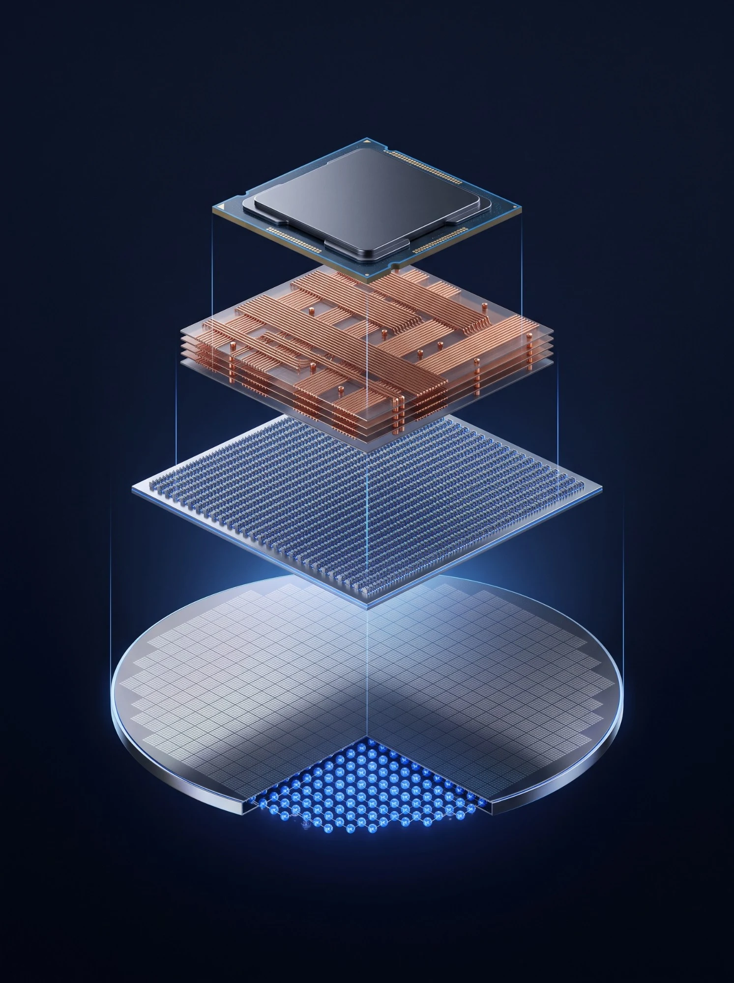
A high-quality substrate is the foundation every chip is built on. When that foundation is strong, you can build far more complex structures with far less chance of failure.

Powered by Digital Twin Technology

Our digital twin technology improves that foundation before a single ingot is grown, testing process changes in simulation so substrate quality is more predictable run to run.

Exploded view of a chip: a single-crystal wafer at the base, then active transistor layers, copper interconnect layers, and the finished chip on top.
EXPLODED VIEWBUILT FROM THE SUBSTRATE UP
Core Capabilities

Supported Manufacturing Methods
Powered by AI Simulation

Bridgman - Stockbarger & Vertical Gradient Freeze

AI-driven control of the temperature gradient through the freeze, including high-pressure VGF for indium phosphide. Our primary area of competence.

Gallium Arsenide (GaAs)Indium Phosphide (InP)Compound Semiconductors

Czochralski Process Scaling

Machine learning models that help calibrate rotation and withdrawal rates for higher single-crystal yield.

Silicon (Si)Germanium (Ge)

Kyropoulos Surface Growth

Predictive temperature control for the production of large-format optical semiconductor materials.

Monocrystalline SapphireLarge Optical Materials
Performance Metrics

Measurable Impact
on Your Production Yields

Years to Weeks

Optimization Timeline

By simulating how temperature and physics alter the outcome before physical testing, we shrink optimization timelines from years to mere weeks.

Higher Output

Increase Process Capabilities

Our AI platform enhances your existing manufacturing processes, unlocking higher production rates and tighter quality control across every growth cycle.

Less Waste

Reduce Waste Through Increased Yield

Fewer failed ingots, less raw material waste. By predicting optimal conditions before each run, we drive yield improvements that compound over time.

Continuous

AI Model Improvement

Our machine learning models continuously update as your facility acquires more real-world data, ensuring your manufacturing yield inherently improves over time.

Get Started

Ready to optimize
your semiconductor yields?

Find out where simulation can move yield in your growth process. The audit is a structured conversation about your furnace, your process and the data you already collect. It takes about an hour and needs no preparation from your team.

Years to WeeksOptimization Timeline
IncreaseProcess Capabilities
Reduce WasteThrough Increase in Yield
ContinuousAI Model Improvement

Built for:

  • Semiconductor Manufacturers
  • Optical Device Creators
  • Research Institutions
  • Industrial Materials Producers